PCB Testing
With boundary-scan and bed of nails to higher test coverage on pcb’s
Due to the increasing demand for compact and energy-efficient components manufacturers package their components as a ball grid array, chip-scale package and quad flat no-leads. Bga’s, csp’s en qfn’s are therefore become indispensable for today's PCBs. Conventional test methods can not accesse there components.
A still frequently used conventional method is, for example, in-circuit test. Some free-moving probes checks if all components are placed correctley on the circuit board and that there are no open or shorted connections. Bga’s, csp’s en qfn’s have only pins on the bottom, and the probes can not.reach these pins.
In addition, engineers often remain hanging on functional tests because they now to use this kind of tests. In case of problems they have a lot of work to find where and why they occur. Often there must first be a software development to audit the board. Functional testing is therefore a costly process that often requires highly educated engineers and brings a longer test period.
High coverage
JTAG boundary scan can offer the solution. This method makes it possible to test PCB’s after assembly. Thereby are Bga’s, csp’s en qfn’s no obstructions. Through special test logic which is built into many modern IC’s, boundary-scan can control if each device is well placed and soldered on the PCB. Because the fault location can be identify quickly and precisely, it is a cost effective solution. Another advantage is that we can test in a earley proces, because there is no firmware needed. It is also possible with JTAG boundary-scan to program different devices on the design, making many traditional tooling unnecessary.
A common misconception is that the use of JTAG boundary scan is a lot of extra work. We only need to extend the design with a pair of passive components for impedance compensation and signal optimization, and with a so-called Test Access Port (TAP) for the connection between the components and the tooling. That's all.
With JTAG boundary-scan is a very high coverage feasible. The optimal result We achieve at the beginning of a project to consider carefully consider the choice of components and the test method. Choose as many chips as possible that meet the
IEEE 1149.1 boundary-scan standard and try to connect the inaccessible devices and networks to unused I/O's of components that do support it, so we can test them anyway.
Furthermore, we can make extra test points to be able to carry analog signals in a so-called extended boundary-scan. This increases the coverage even further and reduces both test time and test costs. It is important to add this test points in in a early schedule level, because later is often no time and space for it.
Rreasonable coverage
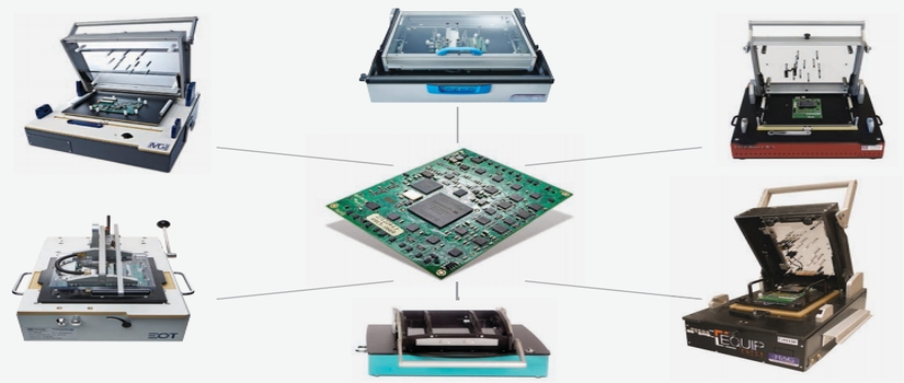
The designs we can test in a fixture. This is a special case in which all the supporting hardware is neatly concealed. The circuit board is in a so-called exchange part, a loose cassette with a bed of nails that we can make customized based on the design data or the Gerber files. When closing the fixture the pins make contacting the tAP and the other test points on the board and there will be a connection to the hardware in the cabinet and from to the tooling. The change parts make it possible to quickly test different types of PCB's and their permanent interface to the fixture we have barely
do any wiring, which drastically reduces the chance of errors. The fixture can be expanded with boundary-scan functionality by adding a JTAG controller as the JT5705, which supports both standard and extended variant.
The controller we can put on an a off-the-shelf JTAG carrier board.This provides all the needed connection to the bed of nails and the fixture. You can also choose to design your own carrier board. Then we must manually add a power and connectors to access the bed of nails. The use of the JT5705 is not tied to a brand fixture.
In cooperation with JTAG Technologies, we have a few years ago developed a test board for training and demonstrations. This JT2156-board is fully configurable and there are several possibilities of setting failures.
Because of involvement in a early stage, we made good desisions about component choces en connections we like to test. Therfore we got on this design with standard boundary-scan a high coverage. Unfortunately, in practice it often happens that the design is ready for production, and there is no possibility to adjust the pcb. It is often still very well possible to test the circuit board through a bed of nails, and to achieve a reasonable coverage with extended boundary-scan. A condition for this is that the design contains at least one boundary-scan component.
Spreading purchase costs
With the company D&D Mechatronics we have developed a fixture that is specifically focused on extended boundary scan, the ProofMaster M19 with JTAG interface. This system has a adjustable power supply, voltage and current are adjustable via a USB connection, from 0 to 20 VDC respectively 0 to 2 A. The power supply is approachable with JTAG Functional Test (JFT) and direct integration into new or existing projects. The ProofMaster M19 also offers the possibility of an ID code to be set on the basis of which is to check whether the correct exchange member is loaded. The exchangeable parts are setup with customer-specific beds of nails and without wiring and are based on the Gerber data of the design that must be tested. The low price for new cassettes eases the step to recycling the fixture, allowing to spread the initial cost of the test box on multiple projects. That makes the ProofMaster M19 also very interesting for smaller PCB order.
Transfer DSW B.V. can realize this entire testing process for you. Please contact our specialists.