VAYO
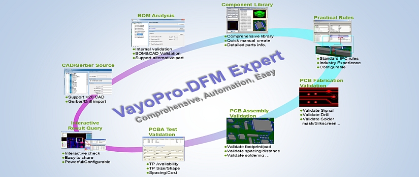
VayoPro-DFM Expert
VayoPro-DFM Expert (Design for manufacturing) is one of the products in the VayoPro® NPI software suite. By overlaying components data with manufacturing requirements, it allows comprehensive design for manufacturability analysis on PCB assembly before manufacturing. It finds defects of the design to ensure perfect match between design and processing capability. It also reduces cost, shortens time to market of new products, and fully enhances product quality and profits. It finds out defect of design at first time to make sure of perfect match between design and processing capability. It turns out to lower the times of trial-producing, reduce cost, shorten time to market of new products, and fully enhance product quality and profits.
Main Commercial Value:
- From design to manufacturing, it is completed in minutes or hours, not weeks or months.
- DFM analysis, improving quality:
- Confirm manufacturability before PCB manufacturing and assembly.
- Improves manufacturing process and quality.
- Improve productivity and efficiency in manufacturing and design.
| Main Project | VayoPro-DFM Expert Introduction | Efficiency Improvement |
|---|---|---|
| R&D design data utilization | Direct use of CAD or Gerber data | 30% - 60% |
| BOM information analysis | Direct processing and analysis on BOM | 30% -60% |
| Simulation of physical components | Simulate physical data in response to different supporters, conduct analog check and matching | 20% - 30% |
| Feedback on DFM | Quickly and accurately generate feedback reports | 10% - 30% |
| Decreases trial-production times | Simulation of software and actual process rules | 50% - 80% |
| Improves quality | Find out design defects and improve it prior to production | 5% - 10% |
| Reduces waste | Reduces time to market and cost | 10% - 25% |
- Worldwide support
- Global, floating, or site licenses available.
Comprehensive DFM Capability:
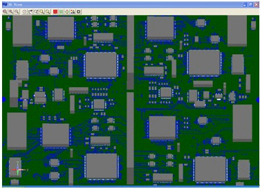
High-performance CAD import of complete graphics data, makes full & effective use of R&D data. DFM Expert is able to directly import and process over 20 CAD formats commonly used in market and perfectly displays PCB location data such as components, net connections, drill, packaging shape, etc.
- CAD types include:
- Altium
- Mentor
- orcad
- Cadence Allegro (including *.brd)
- GenCam
- ZukenCR3000 & ZukenCR5000
- Unidat
- PowerPcb/Pads
- Viscadif
- PCad
- Fabmaster
- Accel
- ODB++
- IPC
- Gencad
- ...and more.
- With flexible and convenient processing of BOM data, detailed information such as manufacturer, manufacturers part number, size and electrical specifications of component and PCB material is analyzed and compared to component library.
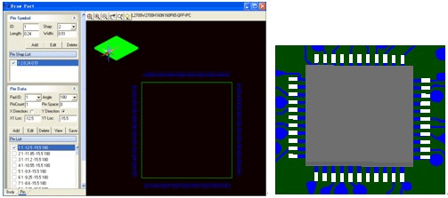
- 3D simulation display of physical components on PCB board.
- Application of process-based operation, automatically confirms procedures to ensure simple and fast use for customers
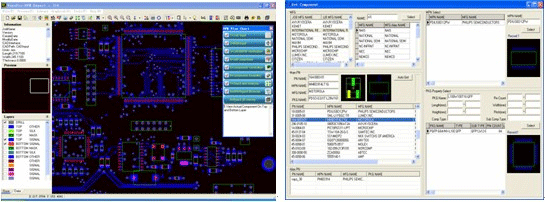
- Comprehensive 3D component library including data of part’s body and pins; supports IPC standard parts library and allows for custom parts to be included as needed
-
The DFM Expert product overlays and compares the CAD data, BOM information and each component data set. There are over 2,000 IPC rules used in determining proper design to ensure the PCBA can be manufactured cost effectively.
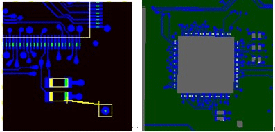
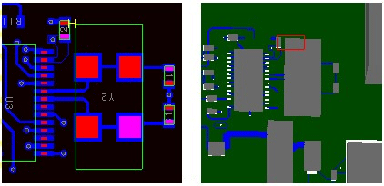
- The DFM analysis covers all electronic and mechanical components and their respective pads or attachment points including all SMT, through-hole, and DIP components as well as fiducials and test points.
- DFM analysis also considers all reflow and wave-soldering processes.
- Analysis considers all component height interactions with other components.
- Rules also consider any expensive or special processes used in PCBA assembly.
- Rules analyze through-hole pin, ensuring proper insertion.
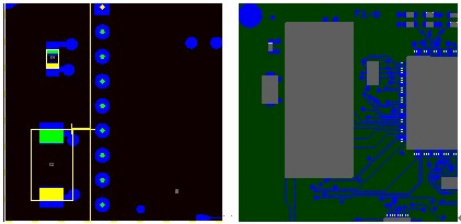
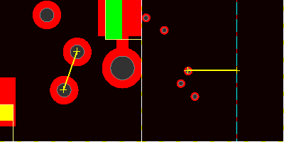
- Reference points are also analyzed for single and multi-board images.
- Test points are analyzed to ensure proper use in testing after assembly, correct pins are used and there is enough space between probes and pins.
- Analysis of RP with SMD and THT components.
- Analysis of:
- Reference Points with components or circuit soldering pad.
- Reference Points with trailing edge or leading edge.
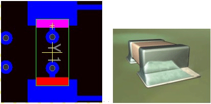
- SMD/THT components packaging
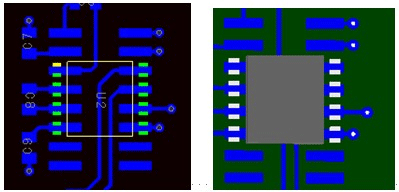
- Analysis of:
- SMD chips and components.
- SMD chips with SMD and TH component
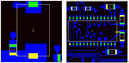
- Analysis of:
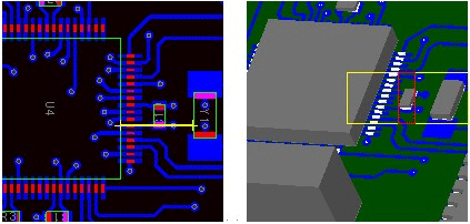
- BGA with high parts around (QFP, SOP, SOT, CONNECTOR…).
- QFP with high parts around (QFP, SOP, SOT, CONNECTOR…).
- SOP with high parts around (QFP, SOP, SOT, CONNECTOR…)
- Analysis of:
- SMD Connector with high parts around (QFP, SOP, SOT, CONNECTOR…).
- Analysis of:
- BGA with TH parts.
- SMD with TH parts
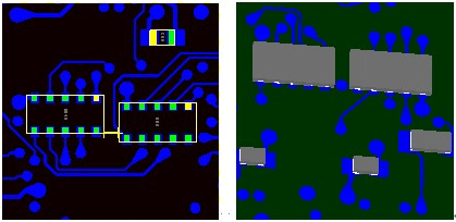
- Analysis of:
- TH parts to TH parts.
- SMD or TH parts in two high components.
- Analysis of:
- SMD pin and pad.
- Analysis of:
- Comp 2 Hole.
- Ppin 2 Hole.
- Cpin 2 Hole.
- Analysis of:
- Analysis of bottom side for top side parts.
- Analysis of:
- SMD pin pitch.
- THT pin to drill.
- SMD to transmission edge or loading edge.
- THT to transmission edge or loading edge.
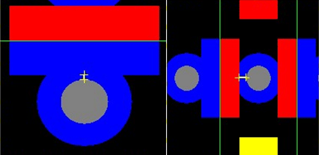
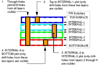
- Drill Check Options (Refer to schematic below).
- Through-hole: drill-holes from all layers (1).
- Blind hole: drill-holes from top or bottom layers (2, 4).
- Buried hole: drill-holes from layer 2 through layer 5 (3).
- Analysis of:
- TH and top side buried hole
- TH to TH
- TH to buried hole
- internal TH to blind hole
- internal TH to buried hole
- internal blind hole to buried hole
- Test point/TP Check.
- Analysis of:
- TP on net.
- TP size.
- TP with circle shape.
- TP to PCB edge.
- TP to SMD parts body.
- TP to TP.
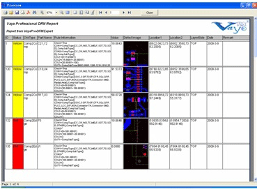
- Professional report on manufacturability analysis with detailed reports. Supports multiple data formats such as:
- EXCEL.
- PDF.
- HTML.
- XML.
- Text.
- 360° view of PCB 3D data.
- ...and more.
For more information we like you to forward to the Vayo website.