ICD
iCD Stackup Planner
"For Engineers and PCB Designers involved in high-speed design, the iCD Stackup Planner offers unprecedented simulation speed, ease of use and accuracy at an affordable price".
The iCD Stackup Planner features a precision 2D Boundary Element Method (BEM) Field Solver providing customers with the accuracy and simulation speed they need for high-speed PCB Design. Seamless integration with the Altium Layer Stack Manager, allows the transfer of substrate materials for the correct trace impedance and automatic creation of Design Rules for differential pairs and trace routing. Bi-directional Interfaces are also available to other EDA tools.
Impedance is the key factor that controls the stability of a design - it is the core issue of the signal integrity methodology. A properly planned PCB substrate can effectively reduce electromagnetic emissions, crosstalk and improve signal integrity providing a low inductance power distribution network. It can also improve the manufacturability of the product, reduce costs and increase product performance and reliability.
Industry-Leading Accuracy
2D (BEM) field solver precision.
-
Characteristic impedance, edge-coupled and broadside-coupled differential impedance.
-
Relative Signal Propagation with 'Matched Delay Optimization'.
-
Termination Planner - Series Termination based on Distributed System.
-
Unique field solver computation of multiple differential technologies per stackup.
-
Heads-up impedance plots of signal and dielectric layers
- Extensive Dielectric Materials Library - over 31,275 rigid & flexible materials up to 100GHz.
- Interfaces to Allegro, Altium Designer, Excel, HyperLynx, OrCAD, PADS, Zmetrix TDR, Zuken and IPC-2581B.
Industry leading Ease of Use
Start with one of the nine default stackups and rearrange to accommodate your specific design needs by adding or deleting signal, plane and dielectric layers. Dragging and dropping single or multiple layers, will instantly re-calculating the entire multilayer stackup to solve for the desired single-ended, edge-coupled, and broadside-coupled differential impedances.
- Fast - Industry leading impedance-simulation speed-across the entire stackup.
- Accurate - the precision you expect from an industry-leading 2D Field Solver (BEM).
- Easy to Use - quick, intuitive, and easy to learn spreadsheet-like interface, with 9 default stackups.
- Practical - insert specific dielectric materials to simulate the actual materials used by your fabricator.
- Differential Pair Integration - solve impedance for multiple differential technologies per stackup.
- Affordable - from entry-level configurations to unlimited functionality - you can choose the solution that best meets your design needs.
Altium Designer Stackup Planner interface supports Altium Designer. The Altium Designer Stackup Planner interface can be used to import the ICD Stackup Planner substrate directly into Altium Designer. Also the stackup can be modified in Altium Designer and exported back to the ICD Stackup Planner.
Multiple Differential Pair Definition
The iCD Stackup Planner is the first controlled impedance tool to enable field solver computation of multiple differential pair definitions per layer. This allows you to incorporate differential 50/100 ohm Digital, 40/80 ohm DDR3/4, 90 ohm USB, 85 ohm PCIe etc sharing the same layers - a stackup planning and documentation tool that can accommodate your differential impedance planning process right out of the box
PlannerDielectric Materials Library
The iCD Stackup Planner FX-HDI edition includes a customizable Dielectric Materials Library, taking In-Circuit Design's industry-leading field solver accuracy one more step toward the actual, fabricated circuit board configuration. By collaborating with your preferred PCB fabricator on their standard, off-the-shelf core, prepreg and solder mask materials, what you calculate - in Stackup Planner FX-HDI - is as close to the real thing as you're going to get. The Dielectric Library Editor comes with a comprehensive library of over 31,500 rigid and flexible core, prepreg, and solder mask materials to 100GHz
ICD Power Distribution Network (PDN) Planner
"Analyze multiple power supplies to maintain low impedance over the entire frequency range dramatically improving product performance and reliability".
The iCD PDN Planner builds on the familiar ease of use of the popular iCD Stackup Planner software that has been used by over 15,000 PCB Designers and Engineers globally since 1996.
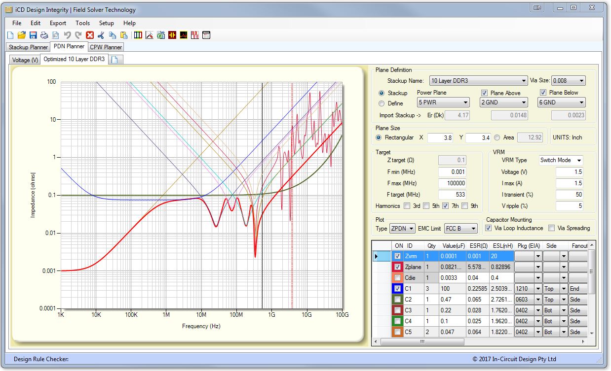
The iCD PDN Planner has the ability to analyze an unlimited number of power supply configurations. A typical high speed multilayer PCB has ten or more individual power supplies that all serve a different purpose and must be regulated to maintain power integrity during high current switching up to the maximum frequency.
PDN EMI Plot
The EMI plot represents the projected maximum radiated noise if a high-speed signal excites the plane resonance at a particular frequency. Plus the applicable EMC standard can be selected from the EMC Limit pull-down menu. In Europe and Australia, the applicable EMC standard is CISPR. The United States complies to the FCC and in Japan the VCCI standard applies.
PDN Planner Capacitor Library
The user may add an unlimited number of bulk bypass and decoupling capacitors. Instantly analyse the Voltage Regulator Module, PCB Substrate - include plane resonance, bulk bypass and decoupling capacitors simultaneously to solve parameters for the desired effective impedance of the Power Distribution Network.
A comprehensive Capacitor Library with over 5,650 readily available SMD capacitors is included listing Value, ESR, ESL, Voltage, Tolerance, Dielectric Material and SMD Package Type ready for insertion into the iCD PDN Planner. Also, capacitors can be entered into the library with the new S-Param Importer.
S-Parameter Capacitor Import to iCD PDN Planner
The Scattering Parameter (S-Param) import to the iCD PDN Planner is via the Touchstone 2-Port (s2p) format. Unfortunately, capacitor manufacturers have quite different styles, of these files, that represent a 2-port model which must be converted to the reflected input impedance S11. The latest trend is for manufacturers to use Touchstone S-Param files to provide capacitor data to their customers. Therefore the S-Param Importer allows iCD software customers to import virtually an unlimited number of capacitors directly from the manufacturer's web site as they are made available.

Alternatively, S-Param capacitors can be imported into the Dielectric Materials Library (DML). It makes sense that if you wish to reuse the S-Param imported capacitors then it is best to import them straight into the library. This is done by opening the DML and selecting 'Import S-Param' from the 'Add capacitor' drop-down menu. There is also a 'Manual Entry' option.
iCD Coplanar Waveguide (CPW) Planner
"Model microstrip Coplanar Waveguides to reduce radiation loss, of high-speed serial links, significantly improving product performance".
The classic coplanar waveguide (CPW) is formed by a microstrip conductor strip separated from a pair of ground plane pours, all on the same layer, affixed to a dielectric medium. The impedance is determined by the ratio of trace width to clearance, so size reduction is possible without limit, the only penalty being higher losses. In addition, a virtual ground plane exists between any two adjacent lines, as there is no field at that point. Hence crosstalk effects, between adjacent lines, are very weak.
A optional Dielectric Materials Library, of over 31,500 rigid and flexible materials up to 100GHz, can optionally be incorporated to further improve accuracy. This can increase accuracy by up to 5%. This is arguably the most comprehensive materials library in the PCB industry. For a complete list of the manufacturers and products included in the library please call our sales. This allows the creation of realistic multilayer stackups using the same core, prepreg and solder mask materials stocked by the PCB Fabricator so, what you calculate is what you get - not approximations!
The CPW offers several advantages over a conventional microstrip transmission line:
- Simplifies fabrication
- Facilitates easy shunt as well as series surface mounting of active and passive devices.
- Eliminates the need for via holes and wraparound (ground plating on the edge of a substrate to provide a low inductance path).
- Reduces radiation loss at very high microwave frequencies.
Coplanar Waveguide Configurations
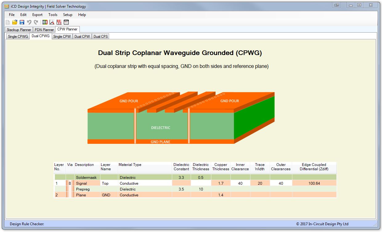
There are five generic CPW structure TABs at the top of the iCD CPW Planner dialog. These represent single and dual (differential) CPW with and without ground reference planes plus a dual Coplanar Strip (CPS) which has no ground reference plane or copper pours.
iCD CPW Planner
- Reduces radiation loss at extremely high frequencies.
- Fast Coplanar Waveguide analysis of five of the most popular microstrip structures.
- Model single and dual (differential) CPWs, with and without ground reference planes, plus a dual Coplanar Strip (CPS) which has no ground reference plane or copper pours.
- Characteristic impedance and edge-coupled differential impedance with solder mask.
- Extensive Dielectric Materials Library - over 31,275 rigid and flexible materials up to 100GHz.
Voor meer informatie kunt u kijken op de ICD website.


